Ova stranica koristi kolačiće (cookies) kako bi osigurala bolje korisničko iskustvo.
Više informacija možete pronaći u Izjavi o kolačićima.


A
A
A
Seminar: Mixed dimensional van der Waals interfaces and their potential applications Dr. Aleksandar Matkovic
Institute of Physics, Montanuniversitaet Leoben, Franz Josef Strasse 18, 8700 Leoben, Austria
14.06.2022. u 15:00h
IRB 1st wing lecture hall
Institute of Physics, Montanuniversitaet Leoben, Franz Josef Strasse 18, 8700 Leoben, Austria
14.06.2022. u 15:00h
IRB 1st wing lecture hall
One of the key advantages that van der Waals (vdW) two-dimensional (2D) materials provide is easy stacking of heterostructures. These have been a wide playground for the researchers in the past decade, allowing for realization of the atomically thin p-n junctions, sub-nanometer channel transistors, harnessing of unique interface and topological states, and many other. Besides stacking of only 2D sheets, organic semiconductors have been also used as additional constituents. Organic semiconductor crystals can be seen as zero-dimensional (0D) vdW materials – with individual molecules as 0D building blocks – and therefore, they can be a very versatile addition to the rapidly developing field of vdW heterostructures.
This talk will explain how small rod-like molecules form needle-like crystalline organic nanostructures on 2D materials through vdW epitaxy. Later we will focus on three particular topics [1-3]:
(a) charge transfer between organic semiconductors and graphene,
(b) photo-assisted charge propagation through organic nanostructures on hBN, and
(c) usage of the self-assembled organic nanostructures as masks for pattering of 2D materials.
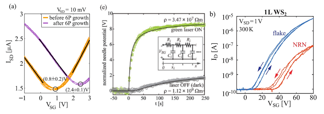
Figure 1: (a) Electrical transfer curves of graphene-FET measured in-situ right before and after deposition of organic molecules [1]. (b) Charging of a single organic semiconductor needle-like crystallite with and without external laser illumination [2]. (c) Electrical transfer curves of a one-layer (1L) WS2 FET before and after patterning of the flake into nanoribbons via organic mask [3].
[1] Matković, A., Kratzer, M., Kaufmann, B., Vujin, J., Gajić, R. and Teichert, C., 2017. Probing charge transfer between molecular semiconductors and graphene. Scientific Reports, 7(1), pp.1-9.
[2] Matković, A., Genser, J., Kratzer, M., Lüftner, D., Chen, Z., Siri, O., Puschnig, P., Becker, C. and Teichert, C., 2019. Light‐Assisted Charge Propagation in Networks of Organic Semiconductor Crystallites on Hexagonal Boron Nitride. Advanced Functional Materials, 29(43), p.1903816.
[3] Aslam, M.A., Tran, T.H., Supina, A., Siri, O., Meunier, V., Watanabe, K., Taniguchi, T., Kralj, M., Teichert, C., Sheremet, E., Rodriguez, R.D., Matković, A., 2022. Single Crystalline 2D Material Nanoribbon Networks for Nanoelectronics, preprint: arXiv:2205.09507v1.