This website uses cookies to ensure a better user experience.
To get more information, please read our Cookie Statement.


Cluster Superlattice Membranes
Our colleagues Davor Čapeta and Marko Kralj, as part of international cooperation, published a paper in the prestigious journal ACS Nano. The paper demonstrates the possibility of forming a free-standing nano-membrane, which consists of a periodic network of metallic nano-clusters on graphene, additionally reinforced with protective layer of amorphous carbon.
Cluster Superlattice Membranes
Tobias Hartl, Moritz Will, Davor Čapeta, Rajendra Singh, Daniel Scheinecker, Virginia Boix de la Cruz, Sophia Dellmann, Paolo Lacovig, Silvano Lizzit, Boris Senkovskiy, Alexander Grüneis, Marko Kralj, Jan Knudsen, Jani Kotakoski, Thomas Michely, Pantelis Bampoulis,
ACS Nano (2020).
DOI: https://doi.org/10.1021/acsnano.0c05740
Hybrid materials that include atomically thin two-dimensional (2D) materials in combination with other nano-materials, provide new functionalities that feature exceptional properties of 2D material (e.g., mechanical strength or conductivity) with functional properties of nano-materials. In this paper, the possibility of preparing a free-standing 2D membrane containing a periodically arranged network of metal clusters is realized: cluster superlattice membrane (CSLM). The cluster network has a well-defined, narrow, cluster size distribution, which can be controlled in the range from a single atom to several hundred atoms in a cluster. Potential applications of CSLM include single electron transistors (SETs), phase formation, and application as electrocatalytic electrodes.
A common property of graphene composites with nanoparticles (graphene nanocomposites) is the absence of crystal arrangement and periodicity. Exceptionally, it is possible to achieve periodic landscaping in a very small area by means of top-down lithography. In contrast, the hybrid material realized in this paper is characterized by the lateral periodicity of the cluster network with a lattice constant of 2.53 nm, which extends over the macroscopic millimeter distances. The key to the formation of such an order lies in the property of epitaxial graphene on Ir (111), which enables the formation of an ordered network of different metal clusters on the graphene moiré superlattice. This structural effect is due to differences in the crystal lattice sizes of the iridium substrate and graphene and offers the possibility of self-organization of nanoparticles on graphene. This system has been very well investigated, but under ultra-high vacuum conditions, where the metal nano-clusters on graphene are protected from various oxidation processes. The key steps towards forming a stable, free-standing membrane with an ordered cluster network are: (a) chemical passivation and structural fixation by deposition of an amorphous carbon protective layer and (b) lift-off of the entire membrane from the Ir (111) substrate and transfer to any other desired substrate or structure. Figure 1 illustrates the steps of preparing a 2D membrane.
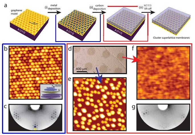
Figure 1: a) The concept for the fabrication of the cluster superlattice membrane. (i) The growth of a cluster superlattice by metal deposition on the moiré on Gr on Ir(111), (ii) embedding of the cluster superlattice with elemental carbon (iii) lift-off from the metal substrate. b) STM topograph of an Ir35 cluster superlattice formed on the Gr moiré after the deposition of 0.4 ML Ir at 300 K. c) The corresponding LEED image acquired at 72 eV. First order Ir (blue) and Gr (yellow) reflections are encircled. They are surrounded by moiré reflections. d) Optical image of the Ir/Gr/Ir(111) sample after the deposition of 7 ML carbon through a shadow mask and annealed to 850 K. e) STM topograph acquired at the regions where carbon is shadowed by the mask, the Ir cluster superlattice has sintered due to annealing to 850 K. f) STM topograph of a cluster superlattice embedded in 7 ML carbon and annealed to 850 K. g) LEED image corresponding to (d) taken at 72 eV. The STM image sizes are 45 nm × 45 nm.
In the process of successful lift-off from the substrate, it was shown that before electrochemical delamination is applied, it is necessary to perform two steps, which on the one hand include heating the material to 850 K and on the other hand intercalation of Eu also at elevated temperature, but at 750 K. Core level photoelectron spectroscopy (XPS), shows that heating to 850 K leads to a reorganization of the chemical bonds in the material. Namely, the deposition of clusters and amorphous carbon on graphene leads to the strengthening of the chemical binding of graphene to iridium due to the rehybridization of graphene orbitals sp2 to sp3. The heating step leads to a redirection of the bonds towards amorphous carbon and a weakening of the bonding of graphene and iridium. Additionally, Eu intercalation leads to a further reduction in the bonds between graphene and iridium.
Finally, after membrane transfer to the transmission electron microscope (TEM) grid, Raman spectroscopy confirmed the membrane transfer, including graphene, whose characteristic peaks are clearly visible in the spectra. The TEM characterization shows a preserved periodic network of metal nano-clusters, where the clusters are imaged in atomic resolution with a well-defined crystal structure and orientation relative to graphene (Figure 2).
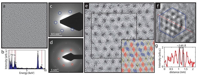
Figure 2. a) Large scale (77 nm × 77 nm) HRTEM image of the cluster superlattice membrane. (b) EDX spectrum of the membrane showing a strong signal correlated to the presence of Ir. (c) and (d) Diffraction images recorded on the membrane, showing the cluster lattice (c) and the Gr lattice (d) spots, taken at different magnifications in reciprocal space. The first order spots are marked with blue and red respectively. (e) A zoom-in HRTEM image (23 nm × 23 nm) of the cluster membrane, showing a closer look of the clusters’ crystalline structure. Inset: sketch of the orientation of the clusters within the black square of panel (e), red indicates cluster epitaxy with the Gr lattice and blue randomly oriented clusters. (f) A zoom-in on a cluster having a lattice that resembles the (111) Ir plane, the image size is (2 nm × 2 nm). (g) The cross section corresponding to the red dashed line of panel (f).