This website uses cookies to ensure a better user experience.
To get more information, please read our Cookie Statement.


Electronic Structure of Quasi-Freestanding WS2/MoS2 Heterostructures
Our PhD student Borna Pielić and several members of SIMAT group, in collaboration with researchers from the University of Siegen and the University of Zagreb, published an article in the prestigious journal ACS Applied Materials & Interfaces, on the growth and characterization of quasi-freestanding WS2/MoS2 heterostructures.
Electronic Structure of Quasi-Freestanding WS2/MoS2 Heterostructures
Borna Pielić, Dino Novko, Iva Šrut Rakić, Jiaqi Cai, Marin Petrović, Robin Ohmann, Nataša Vujičić, Mario Basletić, Carsten Busse, and Marko Kralj, ACS Appl. Mater. Interfaces (2021).
DOI: https://pubs.acs.org/doi/full/10.1021/acsami.1c15412
Growth of two-dimensional (2D) materials under ultra-high vacuum (UHV) conditions allows for an in-situ characterization of samples with a direct spectroscopic insight. Heteroepitaxy of transition metal dichalcogenides (TMDs) in UHV remains a challenge for integration of several different monolayers into new functional systems. In this work, lateral WS2 −MoS2 and vertical WS2/MoS2 heterostructures have been successfully grown on graphene (Figure 1). By means of scanning tunneling spectroscopy (STS) and density functional theory (DFT), the electronic structures of monolayer MoS2, WS2 and WS2/MoS2 vertical heterostructure have been investigated. Weak van der Waals interactions between TMDs and graphene result in relatively large band gaps that deviate only slightly from the DFT-PBE0 calculations obtained for freestanding layers. It is worth noting that other critical energy points also agree well with the DFT. The strong interlayer coupling in WS2/MoS2 vertical heterostructure has been revealed by the analysis of spacing between the states in Γ1 and Γ2.
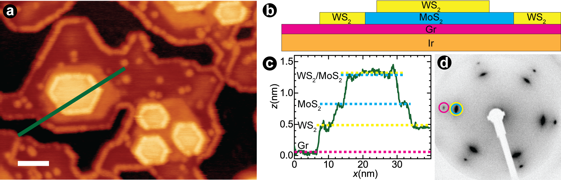
Figure 1: (a) STM image of the WS2 −MoS2 lateral heterostructure and the WS2/MoS2 vertical heterostructure on Gr/Ir(111). Sample bias, tunneling current: 1.2 V, 0.05 nA, scale bar: 10 nm. (b) A schematic sectional view along the green line in (a). (c) STM line pro le along the green line in (a) shows the apparent height difference among four characteristic areas: graphene, WS2, MoS2 and WS2/MoS2 vertical heterostructure. (d) Low energy electron diffraction pattern shows a superposition of WS2 (yellow), MoS2 (cyan) and graphene (magenta) spots marked by circles. Electron energy: 73 eV.
Moreover, a band bending in the vicinity of narrow one-dimensional (1D) interface of the WS2 −MoS2 lateral heterostructure and mirror twin boundary (MTB) in the WS2/MoS2 vertical heterostructure has been investigated. For each system, a position-energy map has been obtained by STS and DFT. For the well-defined interface of the WS2 −MoS2 lateral heterostructure, the type-II band alignment has been confirmed (Figure 2). By using a simple textbook model for pn junctions, the electric field at the interface of 100×106 V/m and the depletion region of 5 nm have been obtained. Such small depletion regions are followed by the relatively large charge densities. Along with the model, the non-linear Thomas-Fermi theory has been used for determination of charge densities. The models show relatively good agreement to experimental data. The grain boundary, specifically the 4|4E MTB, appears between two WS2 islands on top of MoS2 on Gr/Ir(111). The STS line scan characterization reveals that both band gap edges are symmetric around the interface and both exhibit upward band bending. These results indicate that the MTB contains charges defined by 1D MTB band and the polarization charge. By considering the bending of the critical energy points on the band edges, the study suggests that dielectric screening from graphene is affecting mainly the first layer, i.e. MoS2. In such environment, the WS2/MoS2 vertical heterostructure is partially left with its freestanding properties. Quasi-freestanding heterostructures with sharp interfaces, large built-in electric field, and narrow depletion region widths are proper candidates for future designing of electronic and optoelectronic devices.
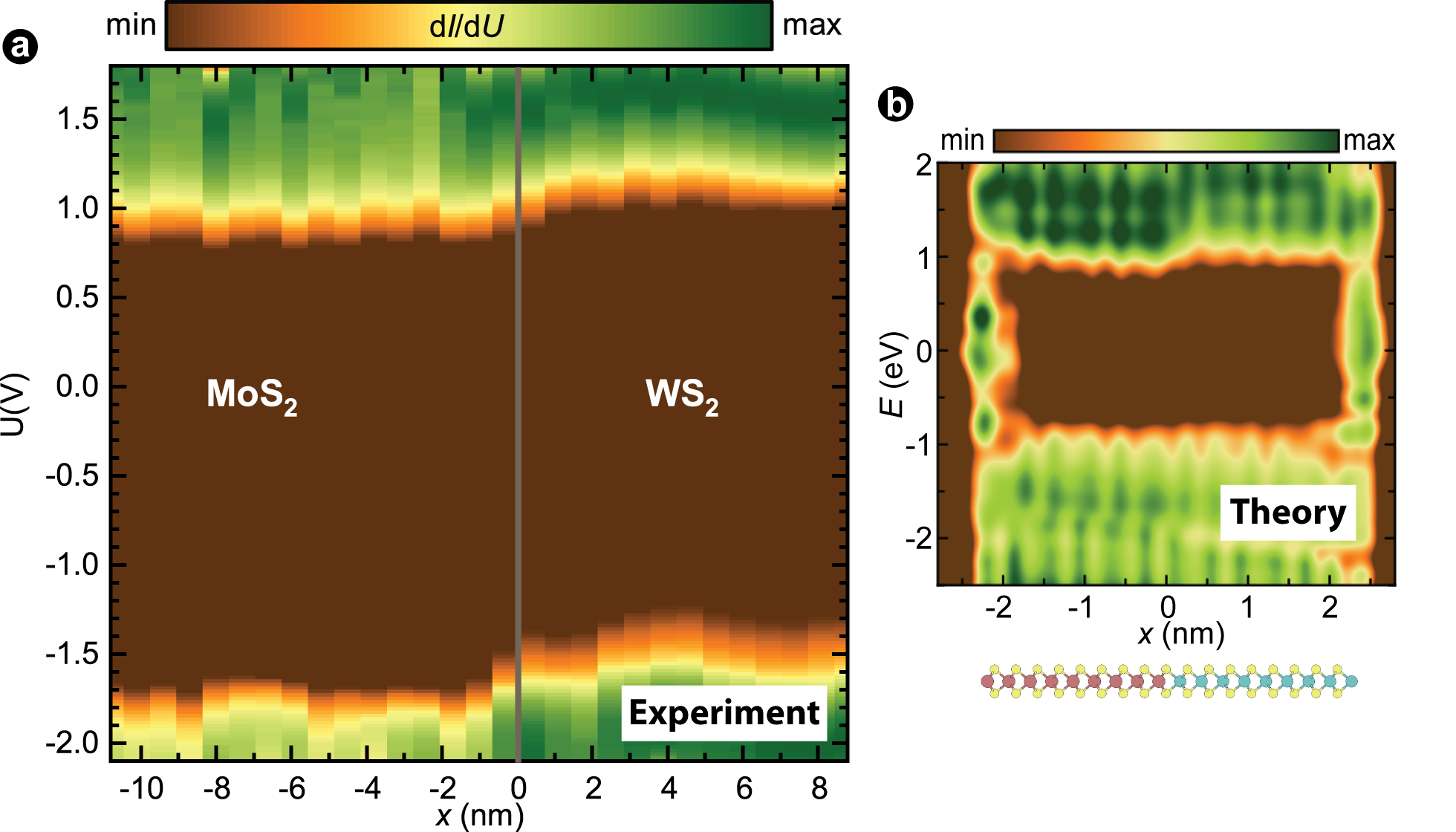
Figure 2: (a) STS line scan across WS2 −MoS2 lateral heterostructure. Gray solid line denotes the position of the interface. (b) Position-energy map with the density of states displayed by the color, obtained by DFT PBE calculation for the unit cell below.