This website uses cookies to ensure a better user experience.
To get more information, please read our Cookie Statement.


Synthesis of large-scale 2D boron
Our colleague Marin Petrović has published a paper in the prestigious journal ACS Nano, demonstrating a scalable route for the synthesis of 2D boron sheets of single-atom thickness. The paper is a result of collaborative work with researchers from the University of Duisburg-Essen and the University of Cologne. The presented findings provide new opportunities for fabrication of large, high-quality layers of emerging 2D materials.
Segregation-Enhanced Epitaxy of Borophene on Ir(111) by Thermal Decomposition of Borazine
Karim M. Omambac, Marin Petrović, Pantelis Bampoulis, Christian Brand, Marko A. Kriegel, Pascal Dreher, David Janoschka, Ulrich Hagemann, Nils Hartmann, Philipp Valerius, Thomas Michely, Frank J. Meyer zu Heringdorf, and Michael Horn-von Hoegen, ASC Nano (2021).
DOI: https://doi.org/10.1021/acsnano.1c00819
Researchers are constantly engaged in the active pursuit of novel materials which enable new scientific findings and technological breakthroughs. For that purpose, high-quality materials are necessary, and their synthesis methods need to be scalable to arbitrarily large dimensions. The synthesis of two-dimensional (2D) materials also faces the same challenges of fabricating large and uniform samples. In particular, scalable synthesis methods of new 2D materials are not fully developed and need to be investigated.
Borophene is a novel 2D material consisting of boron atoms. Unlike graphene which exists only in the form of a honeycomb mesh, borophene can be grown into many crystal structures (i.e., polymorphs) depending on the synthesis substrate. Many polymorphs of borophene have metallic properties, high mechanical strength, and flexibility. In addition to being attractive as an “artificial 2D material”, borophene is potentially applicable for the fabrication of heterostructures with other 2D materials.
In this paper, the authors present a new method for the synthesis of single-layer borophene on an Ir(111) substrate. The method consists of the following two steps: (i) exposing a heated Ir substrate (~1100 °C) to borazine (B3H6N3) vapors in vacuum and (ii) cooling down gradually to the room temperature. At high temperatures, the borazine molecules undergo fragmentation, where hydrogen and nitrogen atoms desorb from the substrate surface. At the same time, B atoms dissolve in the substrate at such high temperatures due to the high solubility of B in Ir bulk. As the solubility of B in Ir decreases with decreasing temperature, the dissolved B atoms are effectively pushed out from the bulk onto the Ir surface during cooldown and self-assemble into borophene monolayer. The process of the B segregation and the growth of borophene layer is shown in Fig. 1, as observed by low-energy electron microscope (LEEM) in real-time.

Figure 1. A sequence of LEEM images showing growth of a single-atom thick borophene layer (bright contrast) on the Ir(111) substrate (dark contrast).
An excellent structural quality of epitaxial borophene formed on the Ir substrate can be confirmed by sharp spots in the low-energy electron diffraction (LEED) pattern in Fig. 2 (a). Moreover, a defect-free structure is observed in the scanning tunneling microscopy (STM) image in Fig. 2(b). It is important to note that this growth method selectively fabricates borophene with single-atom thickness, and the size of the borophene is only dependent on the size of the synthesis substrate. Therefore, this segregation-enhanced epitaxy method can be utilized for producing a large-scale single-layer borophene with excellent structural properties.
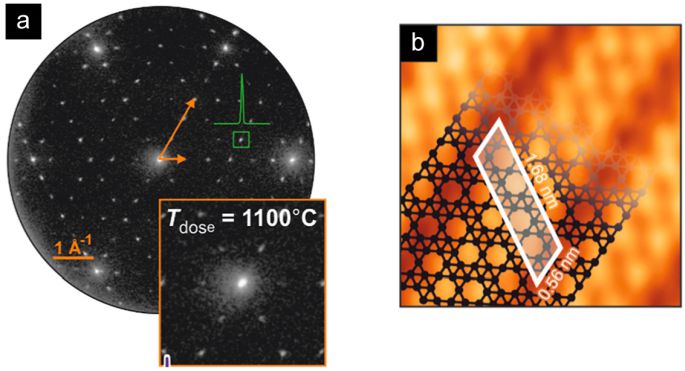
Figure 2. (a) LEED pattern and (b) STM image of borophene on Ir(111). Borophene exhibits a (6×2) superstructure with respect to the Ir surface (with three equivalent 120°-rotated orientations). STM imaging allows identification of a stripe-like pattern which is characteristic for this particular borophene polymorph.