This website uses cookies to ensure a better user experience.
To get more information, please read our Cookie Statement.


Linewidth narrowing with ultimate confinement of alkali multipole plasmon by modifying surface electronic wavefunction with two dimensional materials
Our colleagues Marin Petrović and Marko Kralj, in collaboration with researchers from Kyoto University, published a paper in Physical Review Letters. Intercalation and adsorption of alkali atoms has been utilized for the formation of a 2D material-alkali sandwich, which enabled strong localization of the system’s wavefunction and the formation of a pronounced multipole plasmon.
Linewidth narrowing with ultimate confinement of alkali multipole plasmon by modifying surface electronic wavefunction with two dimensional materials
Shunsuke Tanaka, Tatsuya Yoshida, Kazuya Watanabe, Yoshiyasu Matsumoto, Tomokazu Yasuike, Marin Petrović, and Marko Kralj, Physical Review Letters 125, 126802 (2020).
DOI: https://doi.org/10.1103/PhysRevLett.125.126802
The ability of external electromagnetic field, i.e., light, to propagate in semiconductors and metals is of exceptional fundamental and technological significance, and is important for various applications, such as chemical sensors, photodetectors, photovoltaics, and telecommunications. Realization of the physical process boils down to collective oscillations of electron density within the material, where plasmons are quasiparticles corresponding to those oscillations. To a great extent, plasmons dictate the optical response of metals and semiconductors, and since their wavelengths are much smaller that the wavelengths of the exciting light, they can be spatially localized in materials, for example at surfaces.
Graphene, as a leader in the family of atomically thin materials, has opened new perspectives in research aimed at plasmons due to its semi-metallic character and the ability to finely tune its density of states at the Fermi level. However, optical adsorption for plasmons in graphene is limited to the infrared energy range, while an extension to a broader range is possible only in special cases, e.g. in graphene nanoribbons.
In this paper, epitaxial graphene and hexagonal boron nitride (hBN) on Ir(111) are used as a substrate for special architecture of alkali metal bilayers, where alkali atom intercalation and adsorption enable formation of a structure in which 2D material is “sandwiched” between the two alkali layers. Such structure ensures electronic decoupling of the outermost layer of alkali atoms, which together with 2D material support so-called multipole plasmon with a dipole charge density profile. Dipole character enables direct coupling to external electromagnetic field and a pronounced effect of light absorption in the visible region, which is experimentally observable as a giant and narrow absorption band in sample reflectivity, as visible in Figure. 1.
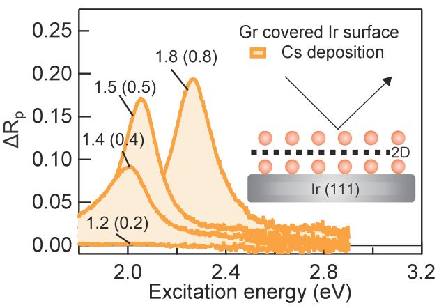
Figure 1. Reflectivity change of Cs/graphene/Cs/Ir(111) structure in dependence of the energy of exciting light, and as a function of Cs coverage (in monolayers, noted for different curves).
Along with experiments which show the effect realized in the structure of alkali layer tailored with atomic precision, time-dependent DFT calculations with jellium model have been employed. Such calculations provides electron density profile at the surface (see Figure 2) and point to the decoupling of the “sandwich” structure from the Ir substrate, which unambiguously confirms the effect of strong multipole plasmon localization within the atomically-thin outer alkali layer accompanied by extreme local amplification of the electromagnetic field by five orders of magnitude.
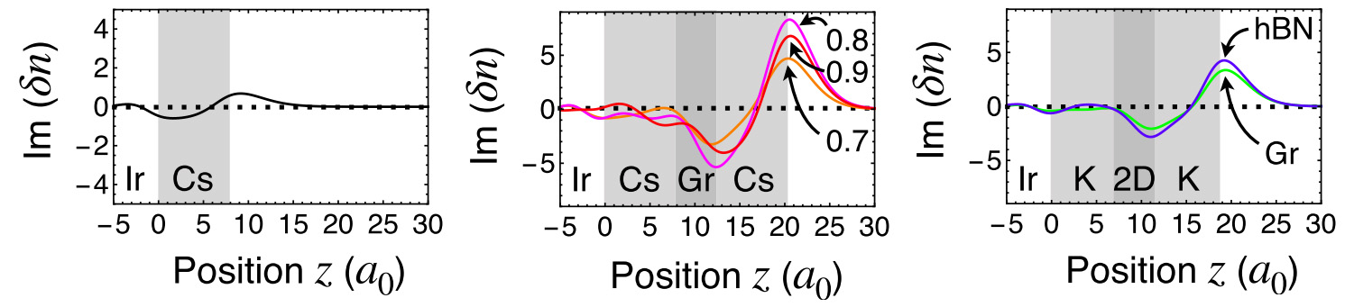
Figure 2. Calculated charge density at Cs/Ir (left), Cs/graphene/Cs/Ir (for various coverages of adsorbed Cs, middle), and K/graphene or hBN/K/Ir (right) samples.