This website uses cookies to ensure a better user experience.
To get more information, please read our Cookie Statement.


Band structure of the thermoelectric SnSe
Our colleague Petar Pervan has together with groups from USA and Italy published a paper in Physical Review Letters on the electron band structure of tin selenide, a layered thermoelectric material.
Band Structure of the IV-VI Black Phosphorus Analog and Thermoelectric SnSe
I. Pletikosić, F. von Rohr, P. Pervan, P. K. Das, I. Vobornik, R. J. Cava, T. Valla, Physical Review Letters 120, 156402 (2018).
DOI: 10.1103/PhysRevLett.120.156403
New developments in electronics and photonics are turning towards materials with fast electron response. Apart from the well-known graphene, phosphorene is also regarded with great interest. Phosphorene is a honeycomb-like two-dimensional structure of phosphorus atoms which makes up the so-called black phosphorus. This almost defect-free structure features a high mobility of charge carriers and a prominent energy gap. The latter enables fine-tuning of electronic properties by eg. changing the gating voltage, which in turn opens the door to building fast transistors, LEDs, lasers, photovoltaic sensors, etc.
Furthermore, the high mobility of phosphorene’s charge carriers is responsible for its high thermoelectric figure of merit, ie. it offers an efficient way to convert the flow of heat into voltage. Unfortunately, phosphorene degrades when in contact with atmospheric oxygen and water. This is why related but stable layered semiconductors are of great interest. Tin selenide, SnSe, is one such material, an isoelectronic and isostructural analog of black phosphorus with the desirably high charge carrier mobility and chemical stability.
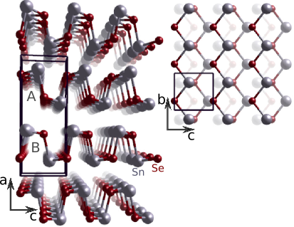
The crystal structure of SnSe viewed (left) along, and (right) perpendicular to the layers. The lower of the two layers contained in the unit cell, A and B, has in the right panel been made nearly invisible.
This work uses angle-resolved photoelectroc spectroscopy (ARPES) to map the electron band structure of SnSe in order to understand its electronic and thermoelectric properties. The new experimental data at low temperatures reveal previously unknown details, among which an anisotropic dispersion as well as multiple hole pockets. Even though the carrier density appears to be somewhat reduced, the highly-mobile, low-mass charge carriers still provide enough conductivity for SnSe’s sizable thermopower.
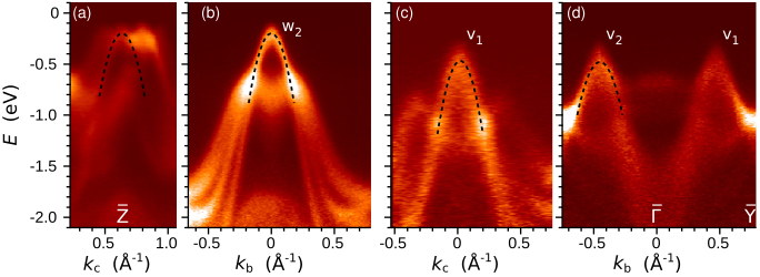
Energy dispersion cuts of the highest-lying pockets in the valence band structure of SnSe along two perpendicular directions in the momentum plane parallel to the layers. Panels (a) and (b) show the holelike pockets centered around Z̄ and (c) and (d) the pockets in the vicinity of Ȳ. The bands are overlaid by parabolic fits used to estimate the effective mass. 34 eV photons were used in (a),(b) and 50 eV in (c),(d).