This website uses cookies to ensure a better user experience.
To get more information, please read our Cookie Statement.


Mechanical manipulation of large scale 2D layers of boron
Members of our SIMAT group, with PhD student Borna Radatović as the leading author, published a paper in the prestigious journal ACS Applied Materials & Interfaces, where they have successfully linked large-scale growth of borophene and its transfer to arbitrary substrates. The quality of the transferred borophene, which is key for future applications, was confirmed in a combined experimental and theoretical approach.
Macroscopic Single-Phase Monolayer Borophene on Arbitrary Substrates
Borna Radatović, Valentino Jadriško, Sherif Kamal, Marko Kralj, Dino Novko, Nataša Vujičić, Marin Petrović. ACS Applied Materials and Interfaces (2022).
DOI: https://doi.org/10.1021/acsami.2c03678
Successful large-scale synthesis of the 2D materials and their mechanical manipulation are some of the key requirements for the utilization of the potential of 2D materials in industrial applications. The same holds for the 2D form of boron, borophene, which is one of the prominent candidates for next-generation devices such as flexible electronics and energy storage. This work successfully connects the synthesis of high-quality single-layer borophene and its subsequent transfer to an arbitrary substrate. Borophene was synthesized via CVD (chemical vapor deposition) growth on Ir(111) monocrystal in vacuum, where its crystal structure and quality were confirmed by electron diffraction. Additionally, the sample was characterized ex situ with Raman spectroscopy and atomic force microscope (AFM) to investigate its ambient stability and topography (Figure 1).
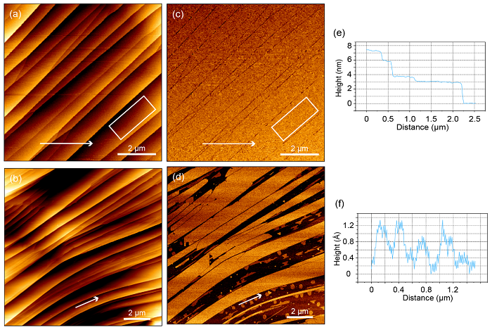
Figure 1. AFM images of borophene or Ir crystal. (a) Region with full borophene coverage. (b) Region with partial borophene coverage. (c) and (d) Phase images of areas depicted in (a) and (b). (e) and (f) Line profiles marked with arrows in (a) and (b).
After initial confirmation of its stability, borophene was transferred to a Si wafer via two-step electrochemical delamination. By exploiting this method, fragments of the borophene with lateral dimensions close to 1 mm were successfully transferred. The target substrate can be arbitrarily chosen, based on specific requirements and demands of each application. The success of the transfer was confirmed with AFM and scanning electron microscope (SEM), showing borophene without any significant contamination and with minimal mechanical damage (Figure 2).
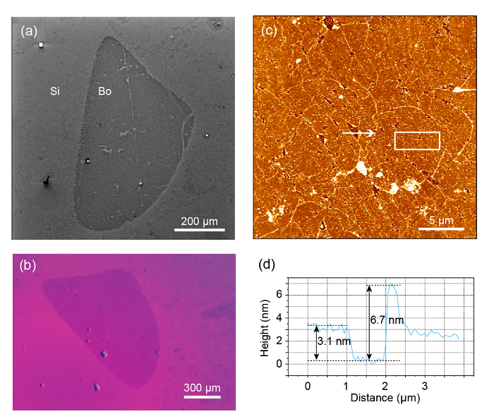
Figure 2. Analysis of borophene after the transfer to a Si wafer. (a) SEM image. (b) Optical image of the largest transferred fragment of the borophene. (c) AFM image of the borophene. (d) Line profile indicated by arrow in (c).
Final confirmation of ambient stability after extraction from vacuum and minimal structural damage of the post-transfer borophene is obtained from comparative Raman spectroscopy of borophene on Ir crystal and on Si wafer. DFT calculations of freestanding borophene provided additional support for identification of individual Raman modes and analysis of similarities and variations between Raman spectra on Ir crystal and Si wafer (Figure 3). This analysis enables standardization of Raman spectroscopy as a fast and efficient method for confirmation borophene quality.
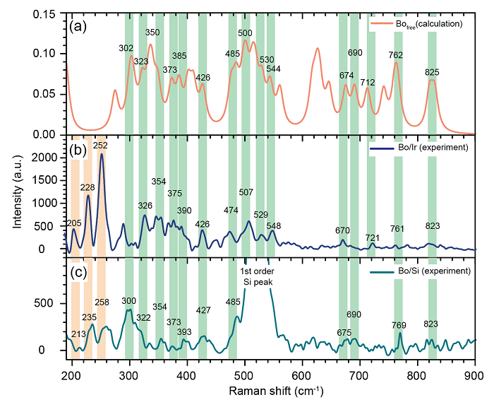
Figure 3. Raman characterization of borophene (a) DFT calculation of Raman spectra of freestanding borophene (b) Measured Raman spectra of borophene or Ir crystal and (c) Raman spectra of borophene on Si wafer. Colored vertical lines indicate common Raman modes.
These results represent a major step towards further utilization of borophene in promising applications, such as energy storage, optoelectronics, and flexible electronic devices, where physical manipulation of 2D boron sheets will be essential.