This website uses cookies to ensure a better user experience.
To get more information, please read our Cookie Statement.


Structural and optical characterization of nanometer sized MoS2/graphene heterostructures for potential use in optoelectronic devices
Members of SIMAT group, with PhD student Valentino Jadriško as the leading author, published a paper in the journal FlatChem, where they present results of MBE synthesis of MoS2/graphene heterostructures, subsequent sample transfer on SiO2/Si wafer as the first step to utilize UHV grown 2D materials and related heterostructures in optoelectronic applications.
Structural and optical characterization of nanometer sized MoS2/graphene heterostructures for potential use in optoelectronic devices
Valentino Jadriško, Borna Radatović, Borna Pielić, Christoph Gadermeier, Marko Kralj, Nataša Vujičić, FlatChem 34, 100397 (2022)
DOI: 10.1016/j.flatc.2022.100397
Two-dimensional semiconductors such as transition metal dichalcogenides combine strong light-matter interaction and rich exciton and valley physics with good chemical stability and scalable fabrication techniques, and are thus excellent prospects for (nano)electronic, optoelectronic, photonic and light-harvesting applications. Scalable fabrication of high-quality samples and their post-synthesis processing and manipulation are still challenging and hinders their adoption for technological application.
In this work, the growth of a high-quality HS of nm size monolayer MoS2 islands on a macroscopic graphene sheet on Ir(111) (6 mm in diameter) and the transfer of the heterostructure to SiO2/Si wafer is presented. UHV two-step MBE synthesis with elemental sulphur to grow MoS2 islands on graphene sheet on Ir(111) is eployed. In-situ LEED and STM measurements confirm the good quality of as-grown samples and quantify the MoS2 coverage, see Figure 1.
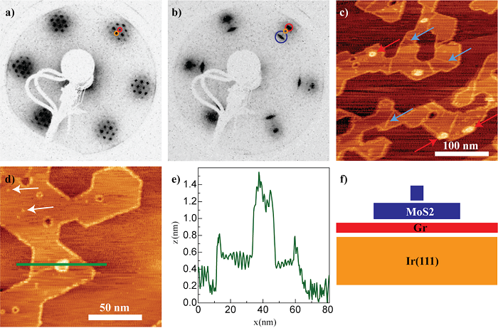
Figure 1. a) and b) LEED patterns of graphene/Ir(111) and MoS2/graphene/Ir(111), respectively. Diffraction spots of graphene (red), Ir (orange) and MoS2 (blue) are marked by circles. c) and d) STM images of monolayer MoS2 islands. Grain boundaries (blue) and point defects (white) in monolayer MoS2, as well as bilayer islands (red), are indicated by arrows. (e) STM line profile along the green line in d). f) Schematic sectional view along the line profile in e).
The sample characterization was done under ambient conditions with AFM. The characteristic surface topography shows that MoS2 islands cover around 22% of the complete surface while the rest of it is clean graphene extended over Ir(111) steps. The average height of the islands is 1 nm proving the ambient stability of the sample. The size of MoS2 islands corresponds to an average of 6 seed segments per island, see Figure 2.
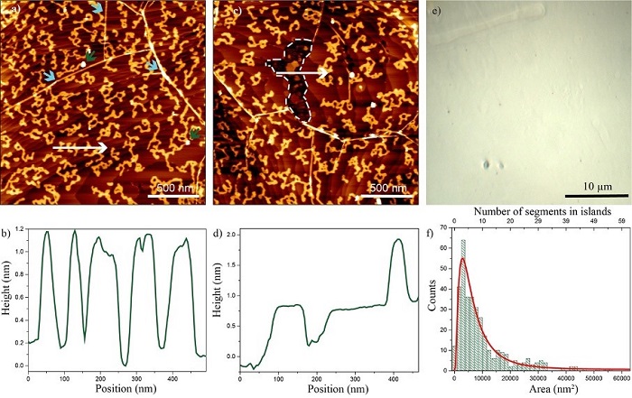
Figure 2. a) AFM image of MoS2 grown on graphene on top of Ir (111) taken after extraction from UHV. b) Height profile along the white arrow in a) which shows thickness of several MoS2 monolayer islands. c) AFM image of a sample area with an etched graphene area outlined by a white dashed line. d) Height profile along the white arrow in c) which shows the thickness of the graphene sheet and one MoS2 island. e) Optical image of sample. f) Distribution of MoS2 islands sizes (histogram) and fit to a log-normal distribution (red line). (For interpretation of the references to colour in this figure legend, the reader is referred to the web version of this article.)
To become independent of the metallic substrate, the heterpstructure is transferred via an electrochemical delamination process. Post-transfer AFM characterization of samples unveils successful transfer of the samples and its stability to ambient conditions. The high quality of the sample is confirmed by its optical response, see Figure 3.
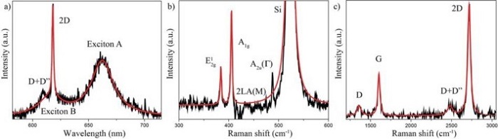
Figure 3. Room temperature PL and Raman characterization. The black line presents the measured spectrum while the red line is the Lorentzian cumulative fit. a) PL spectrum of MoS2 with 2D graphene Raman peak. Raman spectrum of b) MoS2 and c) graphene.
Raman and PL spectra linewidths and intensities indicate interlayer charge transfer between MoS2 and graphene layers, which may serve as a route to the high efficiency optoelectronic devices that could benefit from the combination of the electron-hole photoexcitations in MoS2 (or any other suitable 2D semiconducting material) in combination with the electrically contacted graphene layer. Being nanometer-sized in lateral dimension, the 1T phase metallic edge states in our samples have a substantial impact on MoS2 monolayer behavior than in their micrometer sized counterparts which improves the charge transfer efficiency between MoS2 2H-1T junction.