This website uses cookies to ensure a better user experience.
To get more information, please read our Cookie Statement.


Strain-enhanced large-area monolayer MoS2 photodetectors
Members of our SIMAT group, in collaboration with colleges from 2D Foundry group from Spain, with our former postdoc Borna Radatović as the leading author, published a paper in the prestigious journal ACS Applied Materials & Interfaces, where they show a direct correlation between applied mechanical strain and increase of photoresponsivity, as well as demonstrated endurance of non-encapsulated MoS2 monolayer based strain devices.
Strain-enhanced large-area monolayer MoS2 photodetectors
Borna Radatović, Onur Çakıroğlu, Valentino Jadriško, Riccardo Frisenda, Ana Senkić, Nataša Vujičić, Marko Kralj, Marin Petrović, Andres Castellanos-Gomez
ACS Applied Materials and Interfaces 16, 12, 15596–15604 (2024)
The authors have demonstrated that large-area CVD-grown MoS2 monolayers can be repetitively utilized as a strained photodetector and strain sensor under ambient conditions. Mainly, they determined a direct correlation between applied mechanical strain (ε) and a significant increase in MoS2 monolayer photoresponsivity. As they establish a substantial amplification of photoresponsivity through photocurrent spectroscopy conducted under tensile strains up to 0.9%, demonstrating the potential for enhanced efficiency in MoS2 photodetectors. Investigated devices exhibit high photocurrent and extended response time (τ), both increasing with tensile strain, indicating that photogating mechanisms predominantly govern photocurrent generation. Furthermore, they show the enduring functionality of non-encapsulated MoS2 monolayers as strain-based devices over numerous cycles and extensive time of strain detection under ambient conditions. This resilience underscores the MoS2 monolayer’s potential for further functionalization and diverse applications in flexible electronics such as gas or chemical sensors.
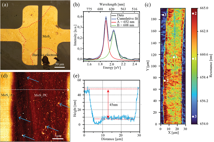
Figure 1. Uniformity characterization in the device channel. (a) Optical micrograph of the MoS2 monolayer transferred on top of PC sheet with pre-fabricated pair of Au electrodes. MoS2 area over electrodes is indicated with a dashed red line. (b) Microreflectance spectrum of MoS2 monolayer in the channel. Exciton A and B Lorentzian fits and cumulative fit are indicated with red, green and blue lines, respectively. (c) PL map of the A exciton resonance of the device channel. Values taken as characteristic A exciton energies for MoS2 in the channel at the PC, MoS2 on the edge of the electrode and MoS2 at Au electrodes are indicated with 1, 2 and 3, respectively. (d) AFM topograph of the sample with no visible cracks in a 30 μm x 30 μm sized region. Blue arrows indicate transfer-induced contamination. (e) The channel line profile taken along the white dashed arrow in (d).
In the first part of the research, the uniformity of the fabricated devices was confirmed by investigating the morphology and optical properties, as shown in Figure 1. After initial measurements, I-V sweeps were performed under ambient with cyclic strain application for a period over 72 h, as shown in Figure 2. Finally, photocurrent spectroscopy was performed to determine the influence of the strain on device performance, as shown in Figure 3.
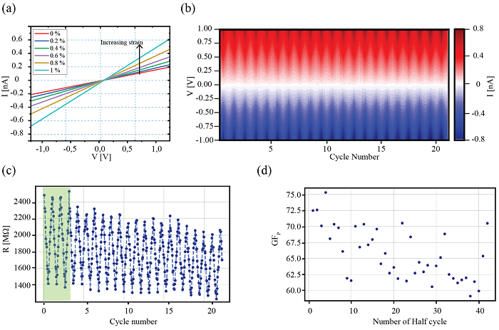
Figure 2. Piezoresistive effect in MoS2 monolayer. (a) I-V characterization under different levels of applied ε up to 1%. (b) Evolution of current versus voltage during 20 bending cycles, where each cycle consists of 21 steps in which strain increases from 0% up to 0.6% and back to 0 %, all in 0.06 % increments, i.e., decrements. The applied voltage is shown on the Y-axis, a cycle number on the X-axis, and a measured current as a colour scale. The red/blue colour indicates the current measured under positive/negative bias. Darker shades of red and blue indicate the highest current (lowest resistance, under 0.6% of applied ε), while brighter corresponds to the lowest current (highest resistance, under 0% of applied ε). (c) Resistance vs. cycle number, with an indicated green rectangle that shows the first three cycles after which pre-strain is partially released. Maximum resistance in each cycle corresponds to 0% of applied ε while minimum to 0.6%. (d) GFP for each new half cycle over the subsequent 20 cycles of bending.
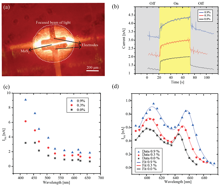
Figure 3. Strain-enhanced MoS2 photoresponse. (a) Optical microscopy image of the device under exposure to light. (b) Photoresponse of MoS2 at light illumination of 645 nm, with the light turned on for 45 seconds and switched off afterwards. Measured current and corresponding double exponential fits are shown for 0.0%, 0.3% and 0.9% of tensile strain. (c) Photocurrent spectroscopy of MoS2 monolayer sheet by exposure to the LED light with different wavelengths, at 0.0%, 0.03% and 0.09% of tensile strain. (d) Higher resolution photocurrent spectroscopy of MoS2 monolayer sheet with exposure to a continuous light source with different wavelengths, at 0.0%, 0.3% and 0.9% of tensile strain. Data shows the energy range in which B (604 nm) and A (645) nm exciton peaks are found and fitted with two Lorentzians.