This website uses cookies to ensure a better user experience.
To get more information, please read our Cookie Statement.


Single-crystalline nanoribbon network field effect transistors from arbitrary two-dimensional materials
Our colleagues Antonio Supina and Marko Kralj, in the scope of bilateral collaboration with researchers from Leoben, published a paper in high-ranking npj 2D Materials and Applications. The study demonstrates universal approach to synthesize high-quality networks of nanoribbons from arbitrary 2D materials.
Single-crystalline nanoribbon network field effect transistors from arbitrary two-dimensional materials
M. A. Aslam, T. H. Tran, A. Supina, O. Siri, V. Meunier, K. Watanabe, T. Taniguchi, M. Kralj, C. Teichert, E. Sheremet, R. D. Rodriguez, A. Matković, npj 2D Materials and Applications 6, 76 (2022)
DOI: 10.1038/s41699-022-00356-y
Graphene nanoribbons (NRs) are considered as a desirable building blocks for information processing in quantum and classical electronics devices. Graphene NRs enable various functionalities including tunable band gap, high current carrying capability, long mean free path, localized spin and topological edge states. In addition, other two-dimensional (2D) material NRs can display edge specific properties such as ferromagnetism, efficient catalysis, and enhanced sensing abilities. Moreover, a recent study about MoS2 NRs demonstrated their potential for spintronics and quantum transport. The development of 2D material NRs is largely driven by the needs in nanoelectronics, where three-dimensional (3D) gate-all-around architectures that employ nanotubes, nanorods, or NRs are considered as the likely solution to the arising scaling challenges.
The bottom-up chemical synthesis routes for precise NR preparation, focus almost exclusively on graphene NRs, facing significant obstacles to develop more complex 2D materials or NR heterostructures. On the other hand, the top-down lithography-based approaches do not offer a straightforward control over NR’s alignment with respect to high symmetry directions of the 2D material. They also cause interface contamination thereby degrading device performance and operation. In this work, collaborators from Montanuniversität Leoben, Tomsk Polytechnic University, Aix Marseille University, Rensselaer Polytechnic Institute, National Institute for Materials Science, and Institute of Physics, tackle the outlined challenges and demonstrate a universal method to fabricate NRs of arbitrary 2D materials, including graphene, hexagonal boron nitride (hBN), transition metal dichalcogenides (TMDCs), and nanoribbon heterostructures with a width ranging from 6 to 100 nm.
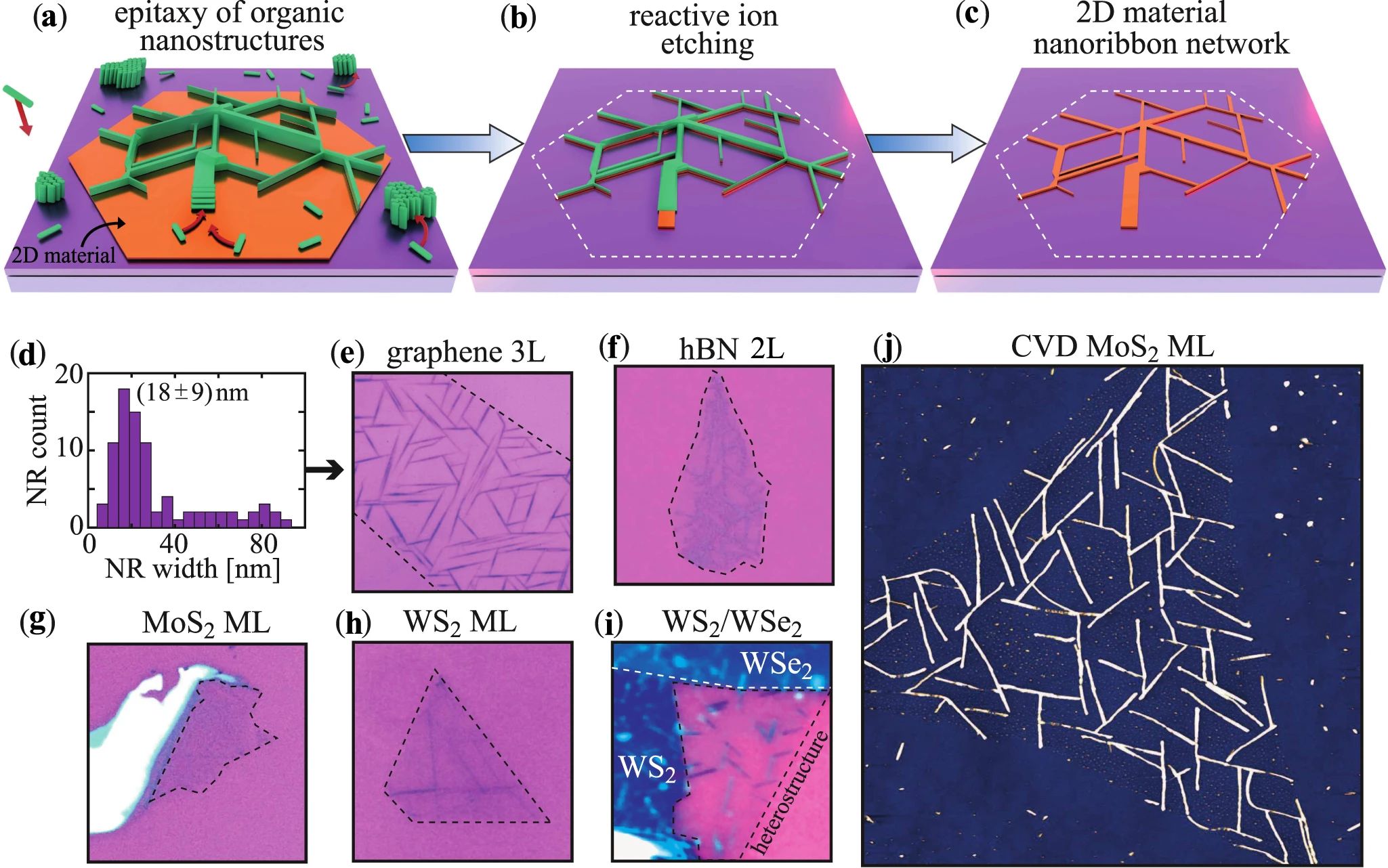
Figure 1. (a)-(c) Schematic illustration of arbitrary 2D material nanoribbon network fabrication process. (d)-(j) Examples of fabricated NRNs based on different 2D materials and heterostructures.
The concept of this work illustrated in Figure 1 relies on well-investigated epitaxy of ordered organic nanostructures which are build of individual small organic molecules, such as 6P (para-sexiphenyl, six phenyl rings single bonded in a linear fashion) or DHTA7 (dihydrotetraazaheptacene, oligoacene derivate with seven rings with nitrogen containing groups). Organic molecules grow on 2D materials via van der Waals (vdW) epitaxy. Namely, the molecules at the interface with the 2D material substrate adopt a flat-lying orientation and align their pi-networks to optimize vdW interaction with the substrate. This leads to self-assembly along high-symmetry directions of 2D materials to form unidirectional nano-needles which are used as a mask through which 2D materials could be etched by oxygen plasma. The final result is crystalline nanoribbon-networks (NRNs) of 2D materials with high edge-to-surface ratio and controlled predominant crystallographic edge-directions.
These NRNs were then further investigated and their electrical performance was tested through directly fabricated field effect transistors (FETs). Besides their inherent single-crystalline nature, NRN-FETs were obtained without any additional transfer steps. TMDC NRN-based devices show outstanding electrical properties, including WS2 and WSe2 nanoribbons. Devices based on graphene NR showed ferroelectric switching due to water adsorption at the ribbon edges. It is important to emphasize that here proposed method allows ribbons that do not suffer from high node resistance between interconnecting NRs, as the networks are ‘carved out’ from single crystals, which was confirmed by in operando Kelvin probe force microscopy (KPFM). To demonstrate the proposed method’s scalability and ultimate control over the NR edge direction, the authors have fabricated predominant armchair and zigzag NRNs from a large-area MoS2 ML obtained by chemical vapor deposited (CVD). Finally, to go step further, a hybrid mixed-dimensional systems were fabricated through decoration of NRNs edges with plasmonic nanoparticles. Such system provides a platform for next-generation optoelectronic and plamsonic sensing devices due to the flexibility provided by implemented method for size tuning of the nanoribbons and the applicability of the process to heterostructures and vertical 2D material p-n junctions.

Figure 2. (a) A schematic diagram of a NRN-based FET utilizing vdW graphite electrodes. Inset of a shows an optical micrograph of a 3L WS2 FET (scale-bar 5 μm). (b)–(d) Semi-logarithmic transfer curves of WS2, MoS2, and hBN-WSe2 FETs before and after patterning the flakes into NRNs. (e) Parallel and fringing capacitance apparent linear electron mobilities at 77 K, for the presented devices.