This website uses cookies to ensure a better user experience.
To get more information, please read our Cookie Statement.


2D boron layer as a nanoscopic diffraction grating
A multimethod investigation of 2D boron sheet – i.e. borophene – on the surface of iridium is reported in a new paper by our colleagues from the SIMAT group with PhD student Sherif Kamal as the lead author. The study, published in ACS Applied Materials & Interfaces, highlights the nanomodulated properties of epitaxial borophene which acts as an electron diffraction grating.
Unidirectional Nano-modulated Binding and Electron Scattering in Epitaxial Borophene
Sherif Kamal, Insung Seo, Pantelis Bampoulis, Matteo Jugovac, Carlo Alberto Brondin, Tevfik Onur Menteş, Iva Šarić Janković, Andrey V. Matetskiy, Paolo Moras, Polina M. Sheverdyaeva, Thomas Michely, Andrea Locatelli, Yoshihiro Gohda, Marko Kralj, and Marin Petrović,ACS Appl. Mater. Interfaces (2023). DOI: https://doi.org/10.1021/acsami.3c14884
In their latest paper, Sherif Kamal, Marko Kralj and Marin Petrović from the Institute of physics, together with international co-workers (Tokyo Institute of Technology, University of Twente, Elettra Synchrotron, University of Rijeka and University of Cologne), report on a combined experimental and theoretical study investigating the structural and electronic properties of an extended monolayer of boron atoms — i.e. borophene — on Ir(111). The research reveals significant nanoscopic and unidirectional modulation in the borophene layer due to non-uniform interaction between B atoms and the underlying Ir atoms, as revealed by the x-ray photoelectron spectroscopy (XPS) and scanning tunneling microscopy (STM) data (see Figure 1). This modulation leads to a stripe-like structure in borophene, functioning as an electron diffraction nano-grating. The scattering of electrons, induced by this grating, results in the formation of replica electronic bands detected in the photoemission spectra of the borophene/Ir(111) system near the Fermi level (see Figure 2). The atomically-thin boron grating, though chemically (re)active and susceptible to atomic-scale modifications, may be easily restored through a dissolution-segregation cycle, during which boron atoms reassemble into a fresh borophene mesh on the surface of Ir(111) substrate.
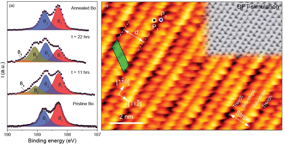
Figure. 1: XPS and STM data acquired after borophene synthesis on Ir(111). (a) B 1s spectra of the borophene/Ir sample recorded immediately after borophene synthesis (bottom), 11 and 22 hours after the synthesis (middle) and after sample annealing to 1100 °C (top). Different components of the B 1s level (B1…4) are indicated. B1 and B2 components are signatures of the variable B-Ir binding. (b) High resolution STM topograph, revealing a stripy structure of the borophene layer, with d denoting the stripe width. The green parallelogram marks the unit cell of borophene. Top right corner: density functional theory (DFT)-simulated STM image of a freestanding borophene.
The findings highlight the scattering capabilities of 2D materials and encourage further exploration of different borophene polymorphs that may exhibit various superperiodicity phenomena. In addition, the study provides a comprehensive understanding of the electronic structure of epitaxial borophene, which is crucial for advancing borophene-based applications. The work demonstrates a straightforward method for fabricating a nanoscopic, highly-ordered system, suggesting its potential use as a template for further functionalization and for implementation into more complex 2D-based heterostructures.
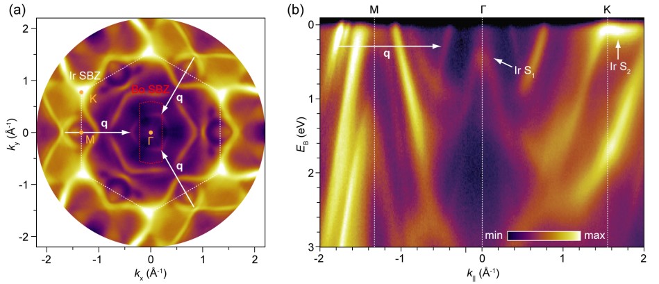
Figure. 2: Angle-resolved photoelectron spectroscopy (ARPES) data of epitaxial borophene on Ir(111). (a) The Fermi surface, within the 1st surface Brillouin zone of Ir(111) (white regular hexagon) and borophene (red elongated hexagon) indicated. Arrows point to borophene-induced replica bands and designate the replication wavevectors q. (b) Map along the M-Γ-K direction with the replication wavevector q and Ir surface states (Ir S1 and Ir S2) indicated.